

Preface. The wood-based world of the future simply won’t have the energy and minerals required not just to make electronic devices, but the precision machine tools to make them. As diesel fuel grows scarce and the economy fails, supply chains will fail, businesses will go bankrupt, and when natural gas is scarce, the electric grid will come down. The very nature of collapse is to go from complexity to simplification. Enjoy all your electronic toys while they last!
And this time is not far away: peak oil happened late 2018 (EIA 2020). It’s past time to preserve knowledge on something more long lasting than microfiche or acid-free paper. Buy books printed on acid-free paper, all the e-books and journals will vanish when the grid goes down.
Alice Friedemann www.energyskeptic.com author of “When Trucks Stop Running: Energy and the Future of Transportation”, 2015, Springer, Barriers to Making Algal Biofuels, and “Crunch! Whole Grain Artisan Chips and Crackers”. Podcasts: Collapse Chronicles, Derrick Jensen, Practical Prepping, KunstlerCast 253, KunstlerCast278, Peak Prosperity , XX2 report
***
How Motherboards Are Made (in 2004)
Without a doubt, motherboards are the most complex and essential part of the modern PC. Not only do they hold the chipsets that pass data from peripherals, drives and memory to the processor, they also provide slots and ports for all your other system components and the circuits through which all data must pass. Perhaps surprisingly then, motherboards get very little respect in the computing press as compared to other components. They are perpetually the team player and not the star of the show, and are generally priced as such.
With this in mind, it’s surprising to learn the amount of work and machinery involved in manufacturing a single motherboard. We’d vaguely imagined some sort of stamping process where all components are slapped onto the bare board in one step and soldered, before being boxed in a big room full of bored workers. Sure there’d have to be some testing, but how intense could it be?
As PCSTATS recent trip to Gigabyte’s Nan-Ping factory in Taiwan showed us last summer during Computex 2004, there’s a lot more to it. In fact, producing and testing a single motherboard involves a mind-boggling host of automated machines, people and processes; so we’d like to detail the whole assembly line to give you a feel for how things are really made.
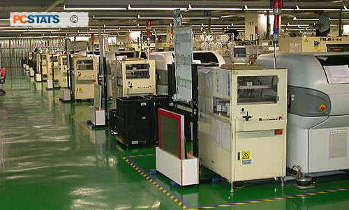
Gigabyte’s Nan-Ping factory is a modern building in rural Taiwan. Built in 1986, this 8-story factory encompasses 45,000 square meters of work space, and includes 18 SMT lines, 10 DIP lines, and 9 Testing lines. Nan-Ping’s capacity is 800,000 motherboards and 400,000 videocards a month. Gigabyte has several other factories in Taiwan and mainland China that each manufacture motherboards, videocards, and other products.
Before entering the factory floor, and especially the SMT (Surface Mount Technology) Lines on the 7th floor of the Nan-Ping factory, workers must go through an air-shower. This small closet-sized enclosure is filled with air nozzles that blast out a stream of air towards three or four occupants at a time, dislodging any dust or particles on their clothes which could cause problems for the sensitive SMT process.
First steps in Motherboard Manufacturing
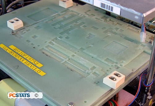
Gigabyte out sources the PCBs (Printed Circuit Boards) it uses for its motherboards to a PCB manufacturer. These arrive already etched with the necessary circuit traces, pre-coloured and pre-drilled with the holes that are needed to insert components like the CPU socket and PCI slots. Other than this though, they are completely bare, containing no components or solder.
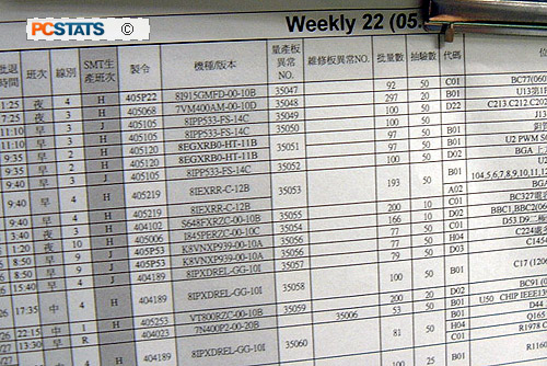
Weekly production sheet identifying the motherboard models
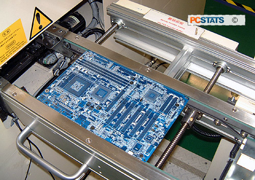
These bare PCB boards are stored on racks and loaded into the automated feeder for the DEK Infinity solder paste printer to start their journey towards becoming completed motherboards.
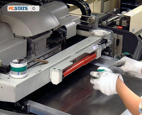
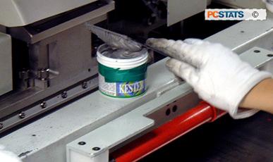
Solder Paste Screen Printing
Before being sent to the SMT (Surface Mount Technology) machines that will mount chips and resistors onto the PCB, each motherboard must be prepared by solder paste printing, a technique which involves spreading solder paste over a nickel sheet, laser cut to correspond to the motherboard being assembled. This nickel sheet ‘screen’ is then moved into the printer and the motherboard positioned precisely under it. The paste is distributed over the screen by the printer so it is squeezed through the holes in the nickel sheet to adhere to the motherboard underneath in precise areas.
|
|
|
|
|
|
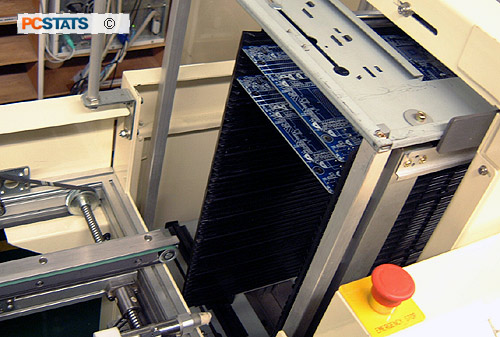
After having the solder paste applied, the bare PCB boards are stacked into an automated vertical storage rack called a PCB Buffer Loader, until ready to be passed through to the SMT assembly machine.
|
|
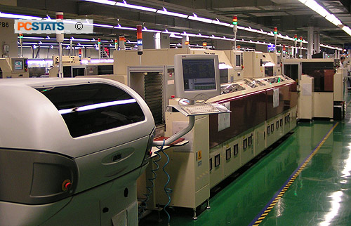
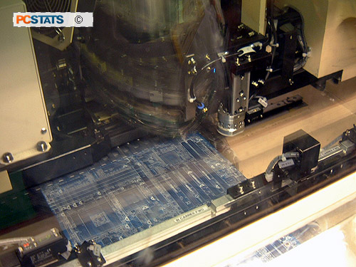
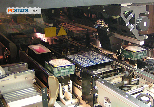
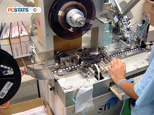
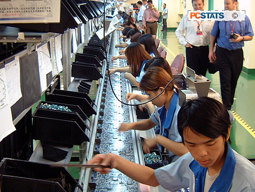
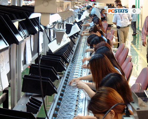
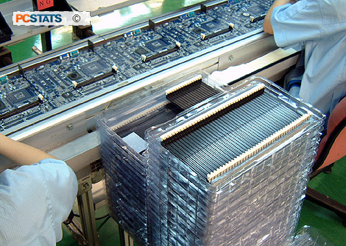
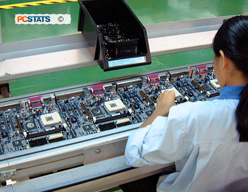
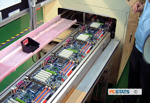
SMT Assembly Line
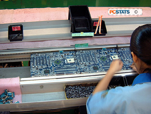
The bare PCBs (Printed Circuit Boards), with solder paste applied in the right places, take the second step towards becoming fully-fledged motherboards here. The SMT (Surface Mount Technology) machines pick and place the tiny resistors, solid-state capacitors and other IC (Integrated Circuit) chips onto the PCB at ultra high speeds. If you look at the motherboard in your computer, some of these small components are no more than 1mm square!
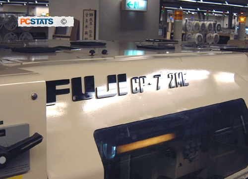
Each board passes through two sets of FUJI CP742 high speed SMT machines, the ‘small pick and place’ and ‘large pick and place’ devices. Each machine in the set adds a few components, from tiny resistors up to the North and Southbridge chips. Belt fed from tape-like cartridges of components, the SMT gear places components like a machine gun, taking as little as an eighth of a second to place a component with exact precision on the PCB.
|
|
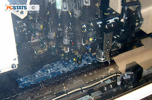
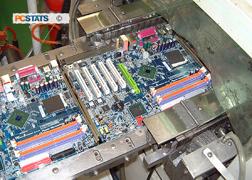
All chipset ICs, plus the BIOS chips and any integrated peripherals (but not their connectors) are added to the top of each motherboard-to-be during this step of the process. The PCB then passes through a Heller 1900EXL hot convection oven to fully melt and set the solder paste, securing the components in position. Motherboards that require components to be placed on the underside of the board are now flipped and sent through the solder screen printing and SMT process again.
|
|
|
|

|
|
|
|
SMT Process Continues
|
|
|
|
|
|
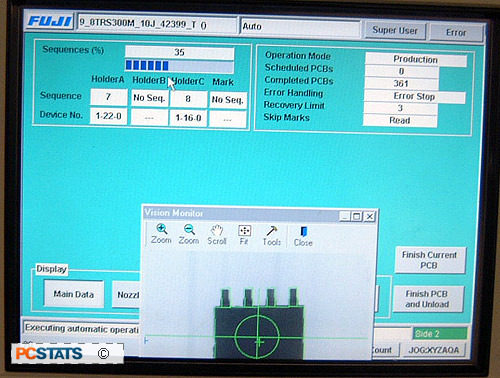
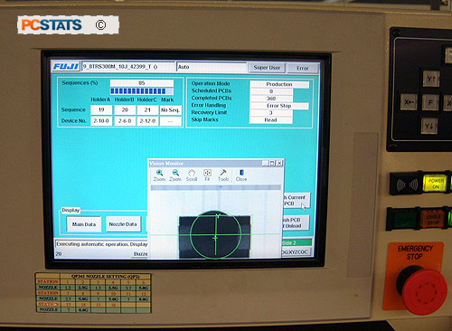
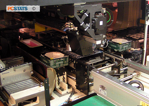
The larger components, Mosfets, audio chips, northbridge chipsets and various other IC’s are placed with the aide of an optical system that ensures tolerances between solder leads and traces are correct. Note that this machine is 35% through its 361st Gigabyte GA-8TRS300M motherboard of the day.
|
|
Pick and Place Chipsets
|
|
Trays of socket 478’s and ATI Radeon 9100IGP chipsets await feeding into the large FUJI QP341 pick and place SMT machines.
|
|

|
|
|
|
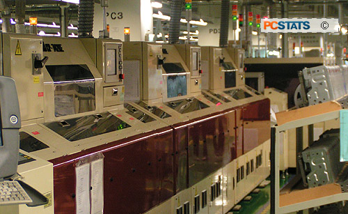
Convection Ovens for PCB
|
|
|
|
With all the IC components placed on the PCB, the motherboards have gone through a Heller 1900EXL hot air convection reflow oven to solder everything in place.
|
|
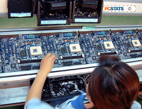
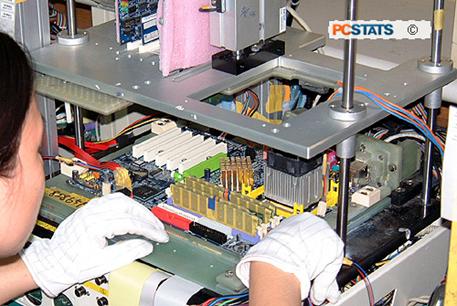
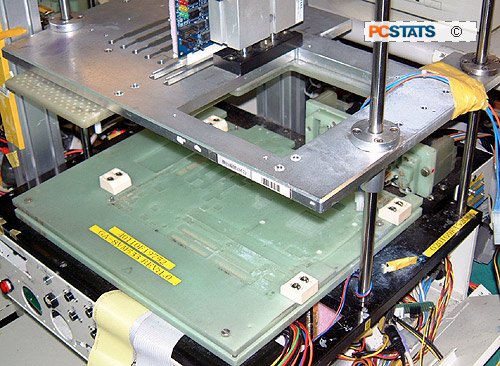
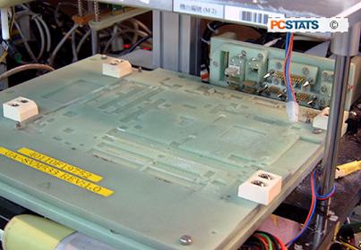
In-Circuit Testing and Visual Inspection
The motherboards now go through an AOI (Automated Optical Inspection) machine which will catch any obvious SMT or soldering defects.
They are then visually inspected by a worker using a plastic mask, so that they can easily spot any missing or misaligned components.
Finally the motherboards undergo an ‘in-circuit test’ which involves testing each motherboard‘s circuit paths, electrical characteristics and the chips that have just been added by applying electrical current to certain specific test points on the board. Each motherboard is placed on a special rack and a testing board is lowered onto it, making contact with the motherboard at specific points. Current is applied, and the results are analyzed by the technician running the station. The whole process takes less than a minute.
|
|
|
|
|
|
|
|
|
|

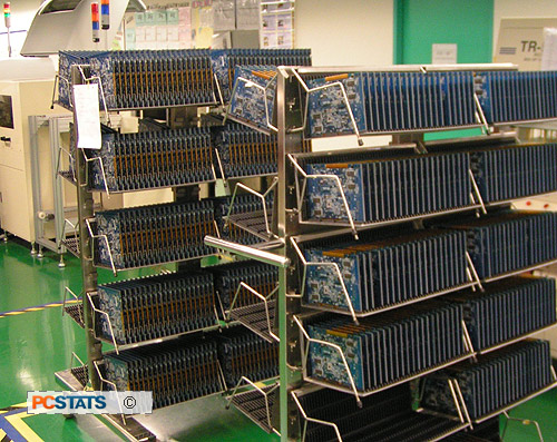
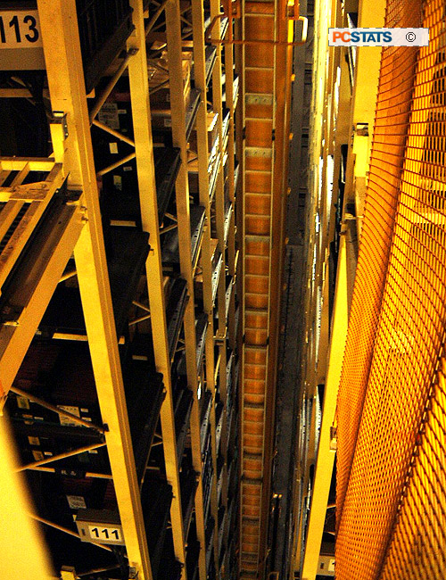
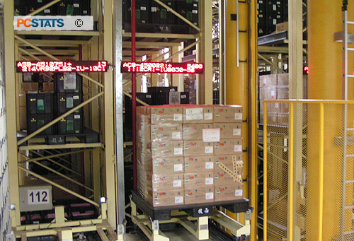
Gigabyte’s Enormous Automated Warehouse
It’s not part of the process, but we should take a minute here to mention the huge automated warehouse that Gigabyte uses to store its various supplies and finished products on site. This vertical storage area is eight stories tall. Eight stories of computer tracked automated pallets that can be raised or lowered to a number of different off loading points, one for each floor. It’s hard to convey the Blade Runner-like effect of this much automated machinery in one place, but these pictures give you a small idea of what it’s like.
|
|
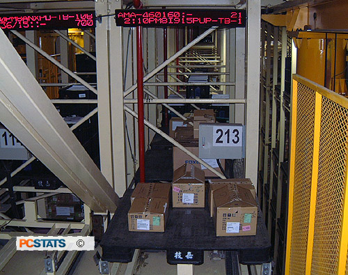
The pallets are loaded by workers into docking stations before automated load handling towers come over to pick up the pallet and ‘file it away in this 8-story warehouse. The process is 100% automated, and pallet are tracked using the numbers visible on the LED display above.
|
|
|
|
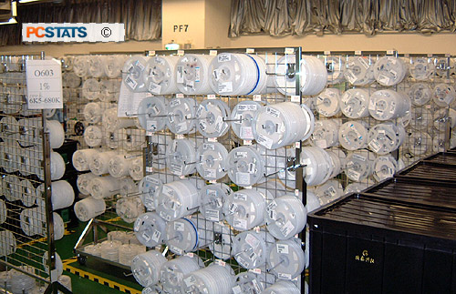
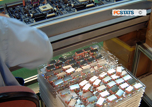
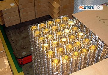
SMT Automated Reel Storage
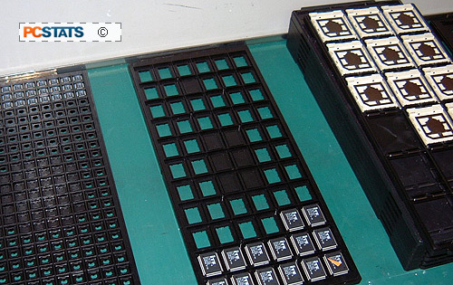
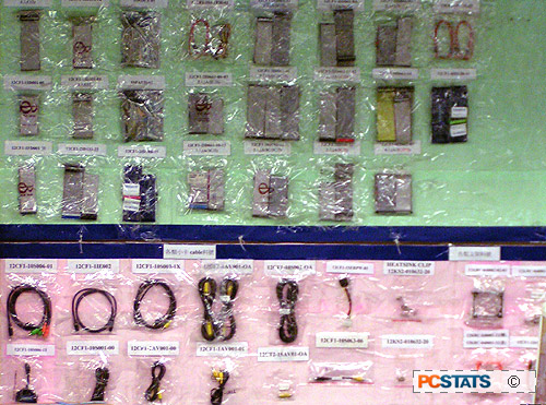
Apart from the warehouse, the production line floors also contained large storage areas, some with racks of component roll cartridges for the SMT machines and some with sealed, moisture-proof cabinets for expensive core-logic components. We also got to see a technician programming BIOS chips prior to their installation.
|
|
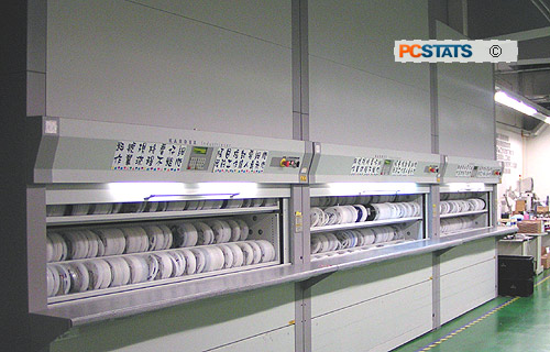
Given the vast number of tiny electric parts that go into a motherboard, we had envisioned buckets of resistors, capacitors, and IC’s. However, given the speed and automation of the factory machines, the time it would take for a machine to pick out a 1 mm square resistor from a pile, oriented it correctly, and place it on the PCB would be too long and inefficient. Thus, all components are stored on film reels, each contained it a little plastic cup. The components are pre-oriented, and the high-speed automated machines can handles these parts with machine-gun like speed.
|
|
|
|
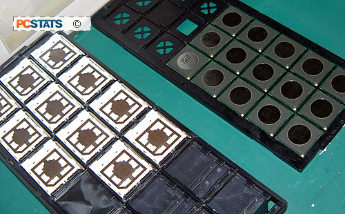
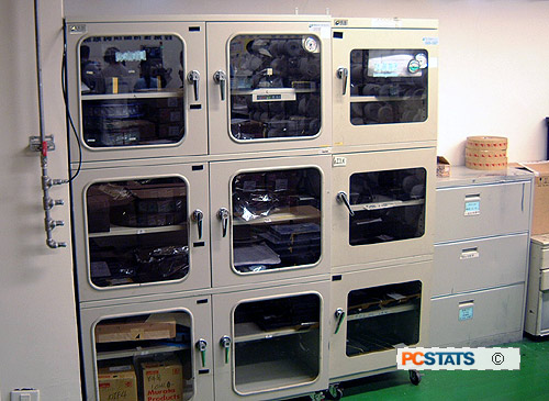
The Expensive Goods
|
|
|
|
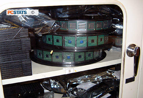
Expensive and sensitive components like Intel i865, i875, 915P, 925X chipsets, south bridges, Radeon‘s and Geforce GPU’s are stored in special moisture free pressurized, temperature controlled cabinets.
|
|

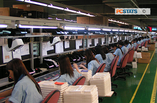
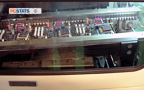
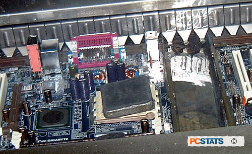
Manual Assembly (DIP) Line
Despite what you might imagine, people are still very much a necessary part of manufacturing motherboards, and not just for testing and Quality Assurance either. The next step in bringing these bare PCB motherboards to life involves a manual assembly line where all the components that need to be plugged into the pre-drilled holes in the board are added.
Every plug and I/O interface is added at this point, from the PCI slots to the CPU socket to the back panel connectors. As well as slots and sockets, capacitors also require anchoring at the bottom of the board, so they are added during this step too. These parts are not soldered to the board during this step, but are simply plugged in, in assembly line fashion.
|
|
|
|
|
|
|
|
Installing Sockets and Ports
|
|
|
|
|
|
|
|
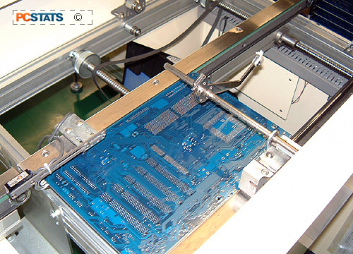
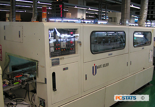
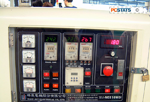
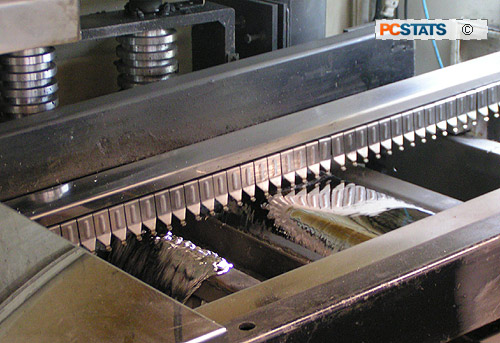
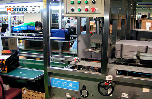
Wave Soldering
The slots, sockets, connectors and capacitors that were plugged into the board on the manual assembly line now need to be soldered to the motherboard. Manual soldering would be too time consuming, so Gigabyte makes use of a special soldering process called wave soldering.
This imposing piece of mechanics is the final step on the conveyor belt that runs through the manual assembly lines. It runs the bottom of each motherboard through a ‘wave’ of liquid solder (induced by flowing the molten solder over a raised ledge) at a precise height, so that the metal leads of the plugged-in components are coated with solder. Each board passes through this wave for 2-4 seconds, after which it is allowed to cool naturally so the solder can solidify around the contacts.
|
|
|
|
Larger sockets sometimes have a tendency to float up a little, so small lead weights are used to hold these sockets down.
|
|
Flowing Over The Molton Solder
|
|
|
|
|
|
|
|
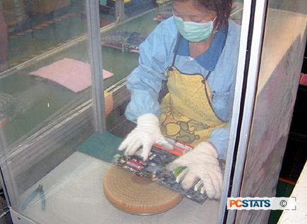
Buffing and Cleaning
The almost-completed motherboards are manually buffed and brushed to smooth down the solder joints at the bottom of the motherboard and remove any loose solder. The masked workers who do this thankless job are confined in little cubicles of plastic to prevent stray particles from contaminating the assembly lines.
|
Worst job in the building? Cleaning the motherboards post-solder |
Final Assembly In the next series of steps, workers adds the last couple of necessary components onto the board. Any required chipset heat sinks are added here as well as the plastic CPU retention bracket, and motherboard battery. When this is complete, the boards are sent off to Quality Assurance for testing.
|
|
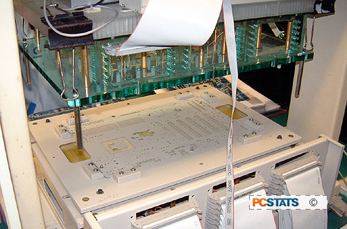
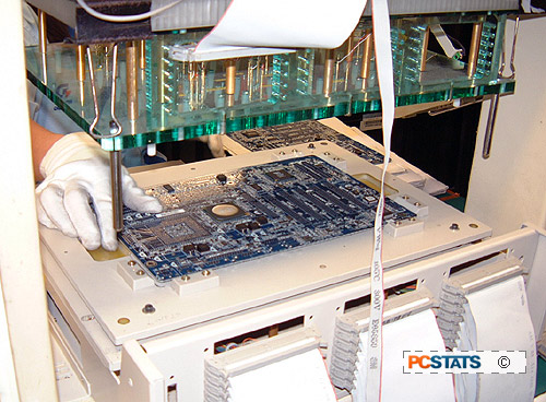
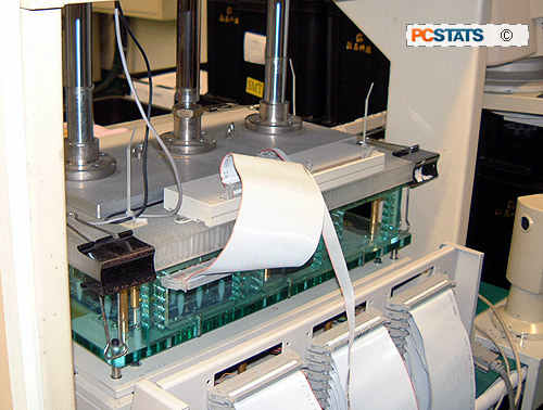
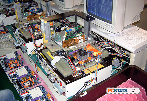
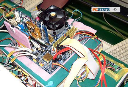
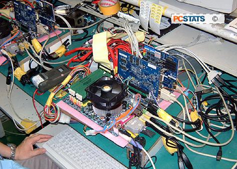
Testing Stage 2: Full Hardware Tests
This test is designed to establish that each motherboard works correctly under ‘normal’ operating conditions. Each testing station has a special rack that is lowered pneumatically, automatically plugging in the test PCI and videocards, and port 80 card while the technician attaches IDE cables, memory and processor and heat sink manually. Interestingly, the test CPU is attached to the bottom of the heatsink with adhesive, and the entire assembly is just placed into the socket in one quick movement.
A second pneumatic connector attaches parallel, serial, PS/2 and USB connectors as well as video sound and networking jacks to the rear I/O panel of the motherboard automatically in one go. The tester adds hard drive, CD and floppy cables attached to components hard mounted to each test station.
|
|
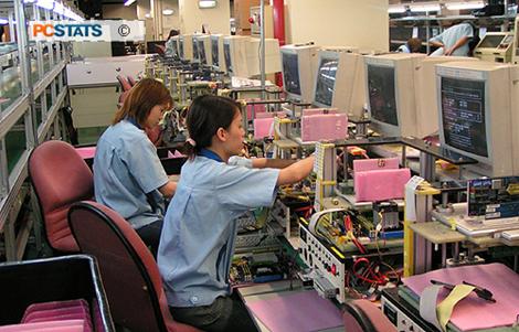
Hooking up each motherboard for testing takes only about a minute. Once set up, the motherboard is powered on and booted into a DOS test program and the functionality of every component and peripheral is confirmed.
Every motherboard is tested for functionality before moving off to the final stage of testing.
|
|
|
|
|
|
|
|
Each worker handles two test stations at once, while the second is being set up the first is left to run a series of automated tests.
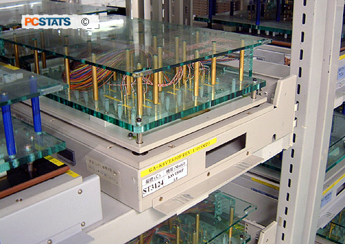
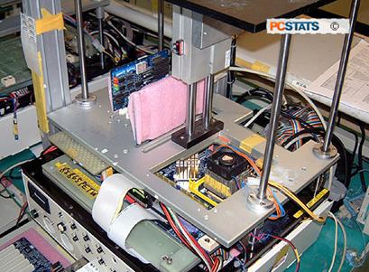
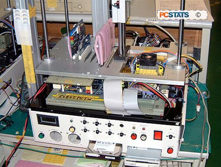
Automated Testing Platforms
|
|
|
|
|
|
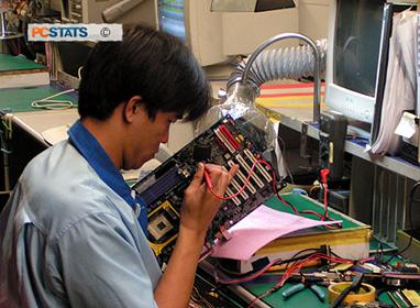
Any boards that fail some tests or need more attention are sent to a manual testing area where technicians test individual components and perform more advanced diagnostics and reworking where necessary.
|
|
|
|
|
|
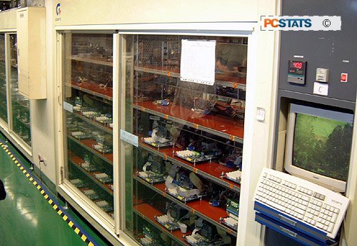
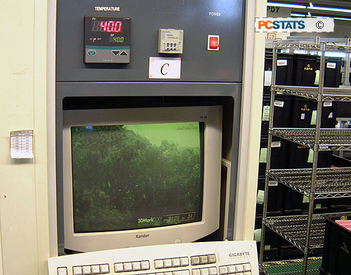
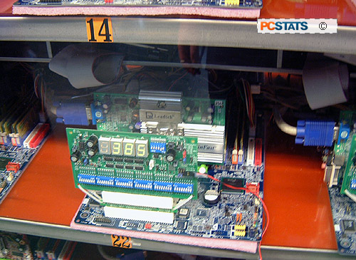
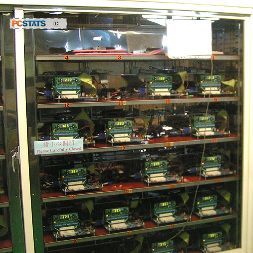
Testing Stage 3: Burn In
The final stage of testing is the stress test. Gigabyte’s Nan-Ping factory has a few huge, temperature controlled glass cabinet where a large number of motherboards can be hooked up with a variety of videocards and stress tested. Each system is run through several hundred loops of 3D Mark 2001 in 40C temperatures. This tests stability under the most grueling of conditions.
|
|
|
|
|
|
|
|
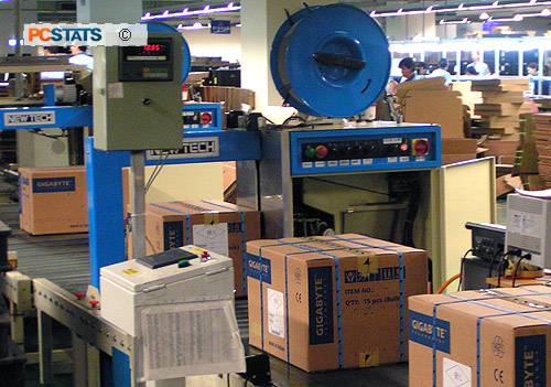
Final Motherboard Packaging
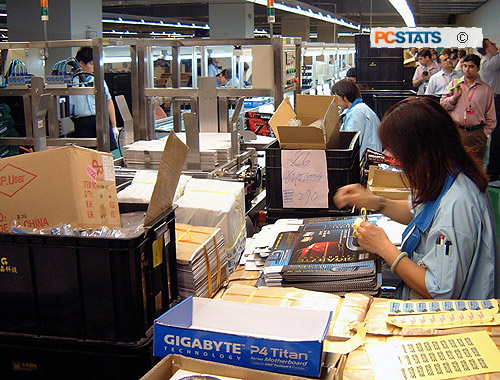
Once the motherboards are fully stress tested, they are ready to be packaged and shipped. Gigabyte, like most manufacturers, orders their motherboard boxes from a separate manufacturer and sends them off to be printed. Once the printed boxes are received, they pass through a machine which folds and shapes them correctly, then it’s down another manual assembly line where workers place each tested motherboard into its box.
In go any promotional stickers, the cardboard divider, antistatic foam, software and other peripherals, then they are sent off to be packed into shipping boxes. The box packing machines are automated, wrapping packing plastic strips around each box faster than the human eye can see!
|
|
|
|
|
|

|
|
|
|
|
|

We hope you’ve enjoyed PCSTATS visual tour of how motherboards are made, and have a better idea of how much work goes into every component of your system! Our thanks goes out to Gigabyte for the unprecedented access they gave PCSTATS to photograph every square inch of the Nan-Ping factory in Taiwan.
References
EIA. 2020. International Energy Statistics. Petroleum and other liquids. Data Options. U.S. Energy Information Administration. Select crude oil including lease condensate to see data past 2017.
Mike D. Feb 5, 2005. How Motherboards Are Made: A Gigabyte Factory Tour. PCSTATS.
http://www.pcstats.com/articleview.cfm?articleid=1722&page=1
3 Responses to Motherboards: too complicated to make after oil